Engineers in the United States and Taiwan say they have demonstrated a promising new twist on nonvolatile memory that’s small enough, miserly when it comes to energy, and works at a low enough voltage that it could boost the abilities of future processors.
The device is a type of phase-change memory, a class of memory that holds information in the form of resistance and changes that resistance by melting and reforming its own crystal structure. The crystal in question, called a nanocomposite superlattice, leads to an order-of-magnitude improvement in the amount of power needed to write a bit, according to research reported last week in Nature Communications. The engineers say this form of phase-change memory (PCRAM) would be particularly useful in future compute-in-memory schemes, which save energy in machine learning by moving less data between memory and processor.
“With switching that low, logic and memory integration are possible.” —Asir Intisar Khan, Stanford
PCRAM has already been commercialized, but it’s not a big segment of the market. It’s thought of as an in-between technology: It’s nonvolatile like flash memory but faster. Yet it’s slower than DRAM, a computer’s main memory, which is volatile. However, an individual phase-change device has the potential to store more data than an individual device of either of the others.
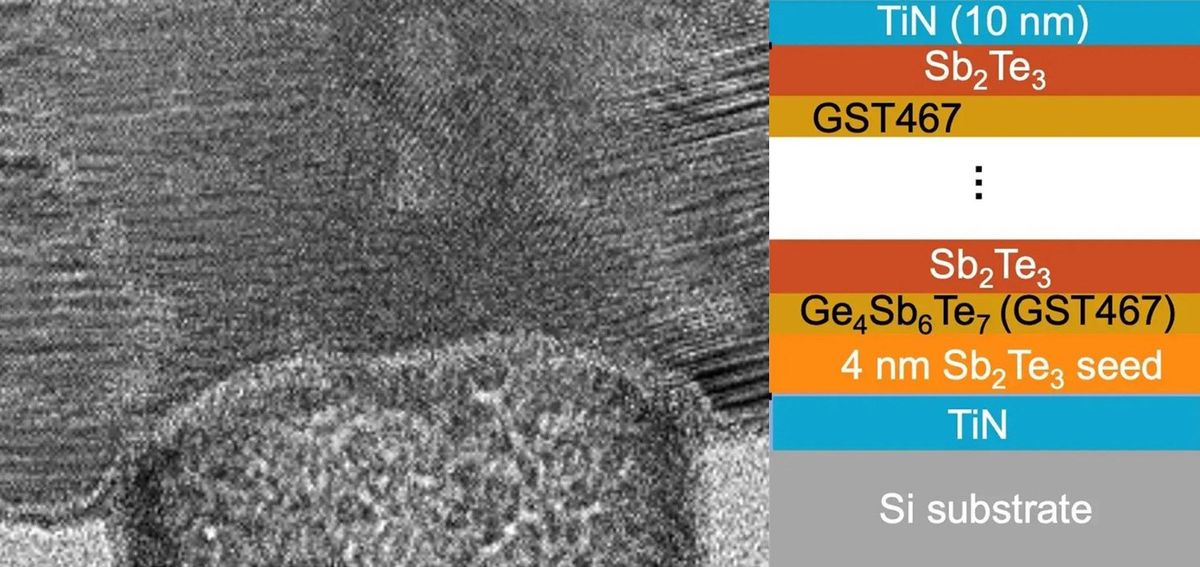
Among the problems holding PCRAM back is that it takes too much current to flip between states. But efforts to fix this have come with trade-offs, such as drifting resistance values. In earlier research, the Stanford University–based part of the team managed to both reduce the current and stabilize resistance. Their answer was a structure called a superlattice, repeating nanometer-scale layers of two different crystal materials. In such a structure, atomic-scale gaps between the layers restrict the flow of heat, so less current is needed to heat the structure and change its phase.
However, those early superlattice devices were too slow to switch and much too large for use in logic chips—about 600 nanometers across. And even though they showed improved energy efficiency, the device’s operating voltage was too high to be driven by CMOS logic, says Stanford postdoctoral researcher Asir Intisar Khan. The team wanted to see if the superlattice concept would work if it was shrunk down to the size required and met other requirements for use in CMOS ICs, and whether doing so would mean the kind of difficult trade-offs that improving PCRAM usually demands.
The goal was a fast-switching, low-voltage, low-power device that was just tens of nanometers wide. “We had to scale it down to 40 nanometers but at the same time optimize all these different components,” says Khan. “If not, industry is not going to take it seriously.”
Getting there required a new material for the lattice: GST467, a compound having a 4:6:7 ratio of germanium, antimony, and tellurium. GST467 was discovered by researchers at University of Maryland, who later collaborated with those at Stanford and Taiwan Semiconductor Manufacturing Co. for use in superlattice PCRAM. The new material is considered a nanocomposite because it has nanometer-scale crystal facets. “These can act as a crystallization template,” explains Xiangjin Wu, a doctoral researcher in the laboratory of Eric Pop at Stanford. Those templates make it easier for the device to regain its crystal structure when a new bit is written.
With a superlattice alternating between layers of GST467 and antimony telluride. Khan, Wu, and their team achieved 40-nm devices that work at 0.7 volts and switch in about 40 nanoseconds while consuming less than 1.5 picojoules. Additionally, the degree of resistance drift was low, it endured about 200 million switching cycles, and it could store data as eight different resistance states for multibit storage per device or for use in analog machine-learning circuits.
“With switching that low, logic and memory integration are possible,” says Khan. The memory cells can be controlled using ordinary logic transistors instead of larger devices meant for I/O, as they are now.
Khan says in addition to further improving the device’s endurance at higher temperatures, the researchers are going to explore what kind of system-level advantages integrating the new PCRAM into logic chips could bring. In particular, it could be useful in experimental 3D chips that are built from the bottom up, rather than from carefully connected stacks of already constructed silicon ICs, as is done in some advanced CPUs and GPUs today. The new PCRAM could be a good fit for integration on top of silicon or other layers because the device’s formation does not require high temperatures that would damage layers beneath it.
Samuel K. Moore is the senior editor at IEEE Spectrum in charge of semiconductors coverage. An IEEE member, he has a bachelor's degree in biomedical engineering from Brown University and a master's degree in journalism from New York University.


