In an exclusive interview ahead of an invite-only event today in San Jose, Intel outlined new chip technologies it will offer its foundry customers by sharing a glimpse into its future data-center processors. The advances include more dense logic and a 16-fold increase in the connectivity within 3D-stacked chips, and they will be among the first top-end technologies the company has ever shared with chip architects from other companies.
The new technologies will arrive at the culmination of a years-long transformation for Intel. The processor maker is moving from being a company that produces only its own chips to becoming a foundry, making chips for others and considering its own product teams as just another customer. The San Jose event, IFS Direct Connect, is meant as a sort of coming-out party for the new business model.
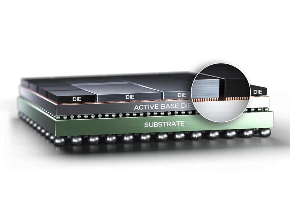
Internally, Intel plans to use the combination of technologies in a server CPU code-named Clearwater Forest. The company considers the product, a system-on-a-chip with hundreds of billions of transistors, an example of what other customers of its foundry business will be able to achieve.
“Our objective is to get the compute to the best performance per watt we can achieve” from Clearwater Forest, said Eric Fetzer, director of data center technology and pathfinding at Intel. That means using the company’s most advanced fabrication technology available, Intel 18A.
3D stacking “improves the latency between compute and memory by shortening the hops, while at the same time enabling a larger cache” —Pushkar Ranade
“However, if we apply that technology throughout the entire system, you run into other potential problems,” he added. “Certain parts of the system don’t necessarily scale as well as others. Logic typically scales generation to generation very well with Moore’s Law.” But other features do not. SRAM, a CPU’s cache memory, has been lagging logic, for example. And the I/O circuits that connect a processor to the rest of a computer are even further behind.
Faced with these realities, as all makers of leading-edge processors are now, Intel broke Clearwater Forest’s system down into its core functions, chose the best-fit technology to build each, and stitched them back together using a suite of new technical tricks. The result is a CPU architecture capable of scaling to as many as 300 billion transistors.
In Clearwater Forest, billions of transistors are divided among three different types of silicon ICs, called dies or chiplets, interconnected and packaged together. The heart of the system is as many as 12 processor-core chiplets built using the Intel 18A process. These chiplets are 3D-stacked atop three “base dies” built using Intel 3, the process that makes compute cores for the Sierra Forest CPU, due out this year. Housed on the base die will be the CPU’s main cache memory, voltage regulators, and internal network. “The stacking improves the latency between compute and memory by shortening the hops, while at the same time enabling a larger cache,” says senior principal engineer Pushkar Ranade.
Finally, the CPU’s I/O system will be on two dies built using Intel 7, which in 2025 will be trailing the company’s most advanced process by a full four generations. In fact, the chiplets are basically the same as those going into the Sierra Forest and Granite Rapids CPUs, lessening the development expense.
Here’s a look at the new technologies involved and what they offer:
3D Hybrid Bonding
 3D hybrid bonding links compute dies to base dies.Intel
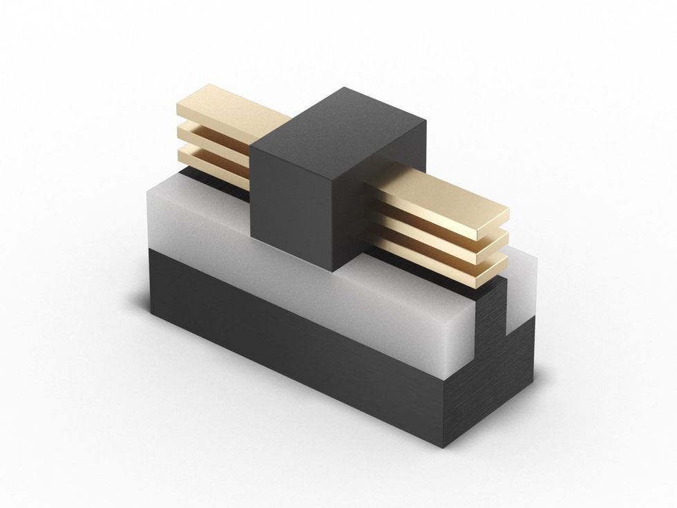
Intel’s current chip-stacking interconnect technology, Foveros, links one die to another using a vastly scaled-down version of how dies have long been connected to their packages: tiny “microbumps” of solder that are briefly melted to join the chips. This lets today’s version of Foveros, which is used in the Meteor Lake CPU, make one connection roughly every 36 micrometers. Clearwater Forest will use new technology, Foveros Direct 3D, which departs from solder-based methods to bring a whopping 16-fold increase in the density of 3D connections.
Called “hybrid bonding,” it’s analogous to welding together the copper pads at the face of two chips. These pads are slightly recessed and surround by insulator. The insulator on one chip affixes to the other when they are pressed together. Then the stacked chips are heated, causing the copper to expand across the gap and bind together to form a permanent link. Competitor TSMC uses a version of hybrid bonding in certain AMD CPUs to connect extra cache memory to processor-core chiplets and, in AMD’s newest GPU, to link compute chiplets to the system’s base die.
“The hybrid bond interconnects enable a substantial increase in density” of connections, says Fetzer. “That density is very important for the server market, particularly because the density drives a very low picojoule-per-bit communication.” The energy involved in data crossing from one silicon die to another can easily consume a big chunk of a product’s power budget if the per-bit energy cost is too high. Foveros Direct 3D brings that cost down below 0.05 picojoules per bit, which puts it on the same scale as the energy needed to move bits around within a silicon die.
A lot of that energy savings comes from the data traversing less copper. Say you wanted to connect a 512-wire bus on one die to the same-size bus on another so the two dies can share a coherent set of information. On each chip, these buses might be as narrow as 10–20 wires per micrometer. To get that from one die to the other using today’s 36-micrometer-pitch microbump tech would mean scattering those signals across several hundred square micrometers of silicon on one side and then gathering them across the same area on the other. Charging up all that extra copper and solder “quickly becomes both a latency and a large power problem,” says Fetzer. Hybrid bonding, in contrast, could do the bus-to-bus connection in the same area that a few microbumps would occupy.
As great as those benefits might be, making the switch to hybrid bonding isn’t easy. To forge hybrid bonds requires linking an already-diced silicon die to one that’s still attached to its wafer. Aligning all the connections properly means the chip must be diced to much greater tolerances than is needed for microbump technologies. Repair and recovery, too, require different technologies. Even the predominant way connections fail is different, says Fetzer. With microbumps, you are more likely to get a short from one bit of solder connecting to a neighbor. But with hybrid bonding, the danger is defects that lead to open connections.
Backside power
One of the main distinctions the company is bringing to chipmaking this year with its Intel 20A process, the one that will precede Intel 18A, is backside power delivery. In processors today, all interconnects, whether they’re carrying power or data, are constructed on the “front side” of the chip, above the silicon substrate. Foveros and other 3D-chip-stacking tech require through-silicon vias, interconnects that drill down through the silicon to make connections from the other side. But back-side power delivery goes much further. It puts all of the power interconnects beneath the silicon, essentially sandwiching the layer containing the transistors between two sets of interconnects.
 PowerVia puts the silicon’s power supply network below, leaving more room for data-carrying interconnects above.Intel
This arrangement makes a difference because power interconnects and data interconnects require different features. Power interconnects need to be wide to reduce resistance, while data interconnects should be narrow so they can be densely packed. Intel is set to be the first chipmaker to introduce back-side power delivery in a commercial chip, later this year with the release of the Arrow Lake CPU. Data released last summer by Intel showed that back-side power alone delivered a 6 percent performance boost.
The Intel 18A process technology’s back-side-power-delivery network technology will be fundamentally the same as what’s found in Intel 20A chips. However, it’s being used to greater advantage in Clearwater Forest. The upcoming CPU includes what’s called an “on-die voltage regulator” within the base die. Having the voltage regulation close to the logic it drives means the logic can run faster. The shorter distances let the regulator respond to changes in the demand for current more quickly, while consuming less power.
Because the logic dies use back-side power delivery, the resistance of the connection between the voltage regulator and the dies logic is that much lower. “The power via technology along with the Foveros stacking gives us a really efficient way to hook it up,” says Fetzer.
RibbonFET, the next generation
In addition to back-side power, the chipmaker is switching to a different transistor architecture with the Intel 20A process: RibbonFET. A form of nanosheet, or gate-all-around, transistor, RibbonFET replaces the FinFET, CMOS’s workhorse transistor since 2011. With Intel 18A, Clearwater Forest’s logic dies will be made with a second generation of RibbonFET process. While the devices themselves aren’t very different from the ones that will emerge from Intel 20A, there’s more flexibility to the design of the devices, says Fetzer.
 RibbonFET is Intel’s take on nanowire transistors.Intel
“There’s a broader array of devices to support various foundry applications beyond just what was needed to enable a high-performance CPU,” which was what the Intel 20A process was designed for, he says.
 RibbonFET’s nanowires can have different widths depending on the needs of a logic cell.Intel
Some of that variation stems from a degree of flexibility that was lost in the FinFET era. Before FinFETs arrived, transistors in the same process could be made in a range of widths, allowing a more-or-less continuous trade-off between performance—which came with higher current—and efficiency—which required better control over leakage current. Because the main part of a FinFET is a vertical silicon fin of a defined height and width, that trade-off now had to take the form of how many fins a device had. So, with two fins you could double current, but there was no way to increase it by 25 or 50 percent.
With nanosheet devices, the ability to vary transistor widths is back. “RibbonFET technology enables different sizes of ribbon within the same technology base,” says Fetzer. “When we go from Intel 20A to Intel 18A, we offer more flexibility in transistor sizing.”
That flexibility means that standard cells, basic logic blocks designers can use to build their systems, can contain transistors with different properties. And that enabled Intel to develop an “enhanced library” that includes standard cells that are smaller, better performing, or more efficient than those of the Intel 20A process.
2nd generation EMIB
In Clearwater Forest, the dies that handle input and output connect horizontally to the base dies—the ones with the cache memory and network—using the second generation of Intel’s EMIB. EMIB is a small piece of silicon containing a dense set of interconnects and microbumps designed to connect one die to another in the same plane. The silicon is embedded in the package itself to form a bridge between dies.
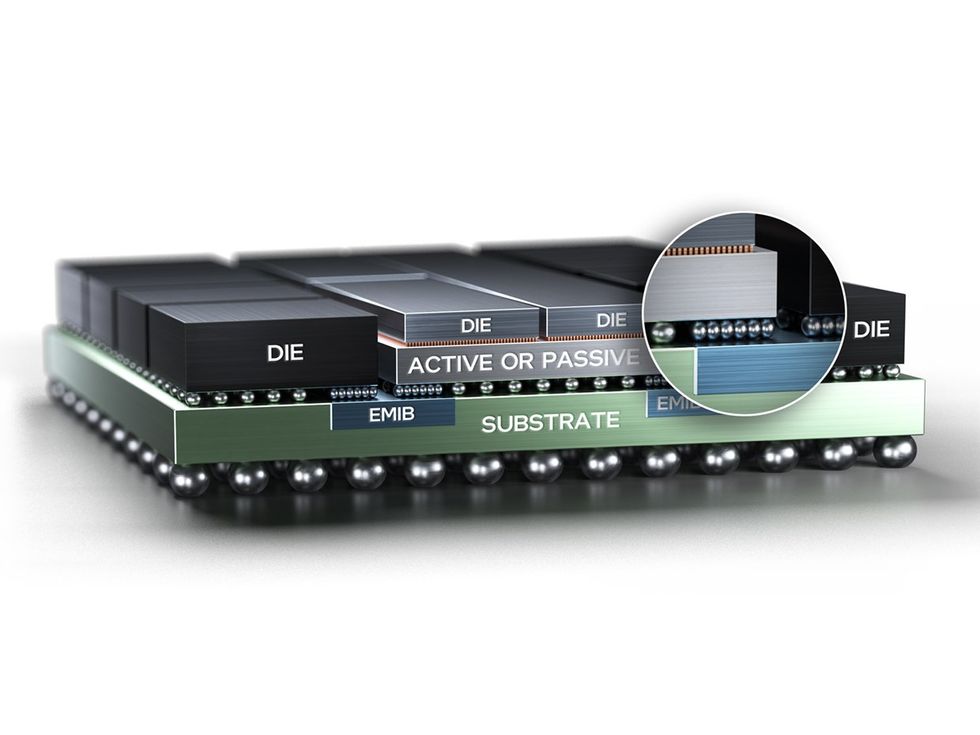 Dense 2D connections are formed by a small sliver of silicon called EMIB, which is embedded in the package substrate.Intel
The technology has been in commercial use in Intel CPUs since Sapphire Rapids was released in 2023. It’s meant as a less costly alternative to putting all the dies on a silicon interposer, a slice of silicon patterned with interconnects that is large enough for all of the system’s dies to sit on. Apart from the cost of the material, silicon interposers can be expensive to build, because they are usually several times larger than what standard silicon processes are designed to make.
The second generation of EMIB debuts this year with the Granite Rapids CPU, and it involves shrinking the pitch of microbump connections from 55 micrometers to 45 micrometers as well as boosting the density of the wires. The main challenge with such connections is that the package and the silicon expand at different rates when they heat up. This phenomenon could lead to warpage that breaks connections.
What’s more, in the case of Clearwater Forest “there were also some unique challenges, because we’re connecting EMIB on a regular die to EMIB on a Foveros Direct 3D base die and a stack,” says Fetzer. This situation, recently rechristened EMIB 3.5 technology (formerly called co-EMIB), requires special steps to ensure that the stresses and strains involved are compatible with the silicon in the Foveros stack, which is thinner than ordinary chips, he says.
For more, see Intel’s whitepaper on their foundry tech.