The Conversation (0)

Davide Comai
DarkBlue1
Scientists have predicted that by 2040, almost 50 percent of the world’s electric power will be used in computing. What’s more, this projection was made before the sudden explosion of generative AI. The amount of computing resources used to train the largest AI models has been doubling roughly every 6 months for more than the past decade. At this rate, by 2030 training a single artificial-intelligence model would take one hundred times as much computing resources as the combined annual resources of the current top ten supercomputers. Simply put, computing will require colossal amounts of power, soon exceeding what our planet can provide.
One way to manage the unsustainable energy requirements of the computing sector is to fundamentally change the way we compute. Superconductors could let us do just that.
Superconductors offer the possibility of drastically lowering energy consumption because they do not dissipate energy when passing current. True, superconductors work only at cryogenic temperatures, requiring some cooling overhead. But in exchange, they offer virtually zero-resistance interconnects, digital logic built on ultrashort pulses that require minimal energy, and the capacity for incredible computing density due to easy 3D chip stacking.
Are the advantages enough to overcome the cost of cryogenic cooling? Our work suggests they most certainly are. As the scale of computing resources gets larger, the marginal cost of the cooling overhead gets smaller. Our research shows that starting at around 10 16 floating-point operations per second (tens of petaflops) the superconducting computer handily becomes more power efficient than its classical cousin. This is exactly the scale of typical high-performance computers today, so the time for a superconducting supercomputer is now.
At Imec, we have spent the past two years developing superconducting processing units that can be manufactured using standard CMOS tools. A processor based on this work would be one hundred times as energy efficient as the most efficient chips today, and it would lead to a computer that fits a data-center’s worth of computing resources into a system the size of a shoebox.
The Physics of Energy-Efficient Computation
Superconductivity—that superpower that allows certain materials to transmit electricity without resistance at low enough temperatures—was discovered back in 1911, and the idea of using it for computing has been around since the mid-1950s. But despite the promise of lower power usage and higher compute density, the technology couldn’t compete with the astounding advance of CMOS scaling under Moore’s Law. Research has continued through the decades, with a superconductingCPU demonstrated by a group at Yokohama National University as recently as 2020. However, as an aid to computing, superconductivity has stayed largely confined to the laboratory.
To bring this technology out of the lab and toward a scalable design that stands a chance of being competitive in the real world, we had to change our approach here at Imec. Instead of inventing a system from the bottom up—that is, starting with what works in a physics lab and hoping it is useful—we designed it from the top down—starting with the necessary functionality, and working directly with CMOS engineers and a full-stack development team to ensure manufacturability. The team worked not only on a fabrication process, but also software architectures, logic gates, and standard-cell libraries of logic and memory elements to build a complete technology.
The foundational ideas behind energy-efficient computation, however, have been developed as far back as 1991. In conventional processors, much of the power consumed and heat dissipated comes from moving information among logic units, or between logic and memory elements rather than from actual operations. Interconnects made of superconducting material, however, do not dissipate any energy. The wires have zero electrical resistance, and therefore, little energy is required to move bits within the processor. This property of having extremely low energy losses holds true even at very high communication frequencies, where losses would skyrocket ordinary interconnects.
Further energy savings come from the way logic is done inside the superconducting computer. Instead of the transistor, the basic element in superconducting logic is the Josephson-junction.
A Josephson junction is a sandwich—a thin slice of insulating material squeezed between two superconductors. Connect the two superconductors, and you have yourself a Josephson-junction loop.
Under normal conditions, the insulating “meat” in the sandwich is so thin that it does not deter a supercurrent—the whole sandwich just acts as a superconductor. However, if you ramp up the current past a threshold known as a critical current, the superconducting “bread slices” around the insulator get briefly knocked out of their superconducting state. In this transition period, the junction emits a tiny voltage pulse, lasting just a picosecond and dissipating just 2 x 10 -20 joules, a hundred-billionth of what it takes to write a single bit of information into conventional flash memory.
![]() A single flux quantum develops in a Josephson-junction loop via a three-step process. First, a current just above the critical value is passed through the junction. The junction then emits a single-flux-quantum voltage pulse. The voltage pulse passes through the inductor, creating a persistent current in the loop. A Josephson junction is indicated by an x on circuit diagrams. Chris Philpot
A single flux quantum develops in a Josephson-junction loop via a three-step process. First, a current just above the critical value is passed through the junction. The junction then emits a single-flux-quantum voltage pulse. The voltage pulse passes through the inductor, creating a persistent current in the loop. A Josephson junction is indicated by an x on circuit diagrams. Chris Philpot
The key is that, due to a phenomenon called magnetic flux quantization in the superconducting loop, this pulse is always exactly the same. It is known as a “single flux quantum” (SFQ) of magnetic flux, and it is fixed to have a value of 2.07 millivolt-picoseconds. Put an inductor inside the Josephson-junction loop, and the voltage pulse drives a current. Since the loop is superconducting, this current will continue going around the loop indefinitely, without using any further energy.
Logical operations inside the superconducting computer are made by manipulating these tiny, quantized voltage pulses. A Josephson-junction loop with an SFQ’s worth of persistent current acts as a logical 1, while a current-free loop is a logical 0.
To store information, the Josephson-junction-based version of SRAM in CPU cache, also uses single flux quanta. To store one bit, two Josephson-junction loops need to be placed next to each other. An SFQ with a persistent current in the left-hand loop is a memory element storing a logical 0, whereas no current in the left but a current in the right loop is a logical 1.
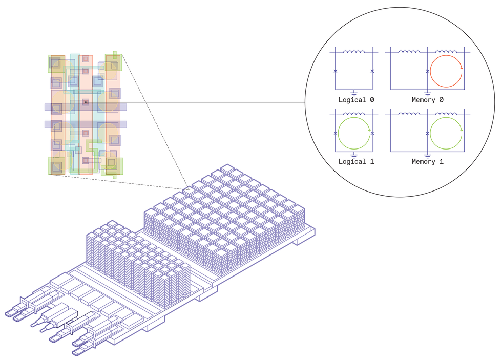 Designing a superconductor-based data center required full-stack innovation. Imec’s board design contains three main elements: the input and output, leading data to the room temperature world, the conventional DRAM, stacked high and cooled to 77 kelvins, and the superconducting processing units, also stacked, and cooled to 4 K. Inside the superconducting processing unit, basic logic and memory elements are laid out to perform computations. A magnification of the chip shows the basic building blocks: For logic, a Josephson-junction loop without a persistent current indicates a logical 0, while a loop with one single flux quantum’s worth of current represents a logical 1. For memory, two Josephson junction loops are connected together. An SFQ’s worth of persistent current in the left loop is a memory 0, and a current in the right loop is a memory 1. Chris Philpot
Progress Through Full-Stack Development
To go from a lab curiosity to a chip prototype ready for fabrication, we had to innovate the full stack of hardware. This came in three main layers: engineering the basic materials used, circuit development, and architectural design. The three layers had to go together—a new set of materials requires new circuit designs, and new circuit designs require novel architectures to incorporate them. Codevelopment across all three stages, with a strict adherence to CMOS manufacturing capabilities, was the key to success.
At the materials level, we had to step away from the previous lab-favorite superconducting material: niobium. While niobium is easy to model and behaves very well under predictable lab conditions, it is very difficult to scale down. Niobium is sensitive to both process temperature and its surrounding materials, so it is not compatible with standard CMOS processing. Therefore, we switched to the related compound niobium titanium nitride for our basic superconducting material. Niobium titanium nitride can withstand temperatures used in CMOS fabrication without losing its superconducting capabilities, and it reacts much less with its surrounding layers, making it a much more practical choice.
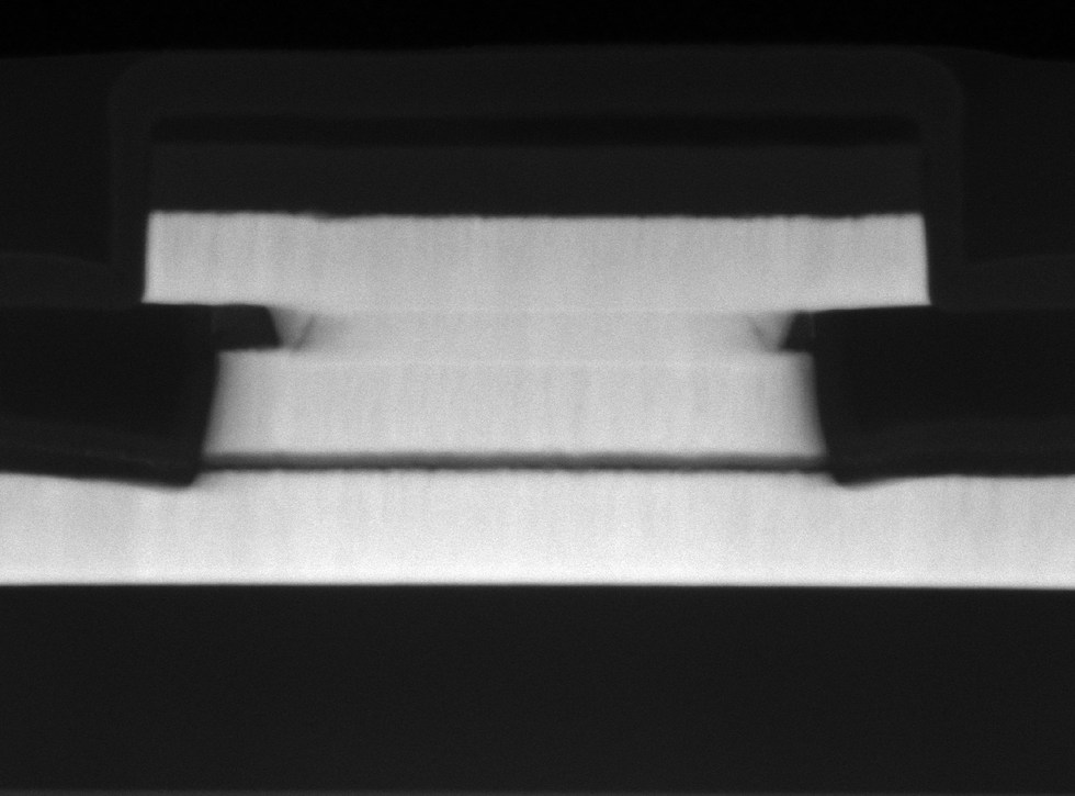 The basic building block of superconducting logic and memory is the Josephson junction. At Imec, these junctions have been manufactured using a new set of materials, allowing the team to scale down the technology without losing functionality. Here, a tunneling electron microscope image shows a Josephson junction made with alpha-silicon insulator sandwiched between niobium titanium nitride superconductors, achieving a critical dimension of 210 nanometers. Imec
Additionally, we employed a new material for the meat layer of the Josephson-junction sandwich—amorphous, or alpha, silicon. Conventional Josephson-junction materials, most notably aluminum oxide, didn’t scale down well. Aluminum was used because it “wets” the niobium, smoothing the surface, and the oxide was grown in a well-controlled manner. However, to get to the ultrahigh densities that we are targeting, we would have to make the oxide too thin to be practically manufacturable. Alpha silicon, in contrast, allowed us to use a much thicker barrier for the same critical current.
We also had to devise a new way to power the Josephson junctions that would scale down to the size of a chip. Previously, lab-based superconducting computers used transformers to deliver current to their circuit elements. However, having a bulky transformer near each circuit element is unworkable. Instead, we designed a way to deliver power to all the elements on the chip at once by creating a resonant circuit, with specialized capacitors interspersed throughout the chip.
At the circuit level, we had to redesign the entire logic and memory structure to take advantage of the new materials’ capabilities. We designed a novel logic architecture that we call pulse-conserving logic. The key requirement for pulse-conserving logic is that the elements have as many inputs as outputs and that the total number of single flux quanta is conserved. The logic is performed by routing the SFQs through a combination of Josephson-junction loops and inductors to the appropriate outputs, resulting in logical ORs and ANDs. To complement the logic architecture, we also redesigned a compatible Josephson-junction-based SRAM.
Lastly, we had to make architectural innovations to take full advantage of the novel materials and circuit designs. Among these was cooling conventional silicon DRAM down to 77 kelvins and designing a glass bridge between the 77-K section and the main superconducting section. The bridge houses thin wires that allow communication without thermal mixing. We also came up with a way of stacking chips on top of each other and are developing vertical superconducting interconnects to link between circuit boards.
A Data Center the Size of a Shoebox
The result is a superconductor-based chip design that’s optimized for AI processing. A zoom in on one of its boards reveals many similarities with a typical 3D CMOS system-on-chip. The board is populated by computational chips: We call it a superconductor processing unit (SPU), with embedded superconducting SRAM, DRAM memory stacks, and switches, all interconnected on silicon interposer or on glass-bridge advanced packaging technologies.
But there are also some striking differences. First, most of the chip is to be submerged in liquid helium for cooling to a mere 4 K. This includes the SPUs and SRAM, which depend on superconducting logic rather than CMOS, and are housed on an interposer board. Next, there is a glass bridge to a warmer area, a balmy 77 K that hosts the DRAM. The DRAM technology is not superconducting, but conventional silicon cooled down from room temperature, making it more efficient. From there, bespoke connectors lead data to and from the room-temperature world.
 Davide Comai
Moore’s law relies on fitting progressively more computing resources into the same space. As scaling down transistors gets more and more difficult, the semiconductor industry is turning toward 3D stacking of chips to keep up the density gains. In classical CMOS-based technology, it is very challenging to stack computational chips on top of each other because of the large amount of power, and therefore heat, that is dissipated within the chips. In superconducting technology, the little power that is dissipated is easily removed by the liquid helium. Logic chips can be directly stacked using advanced 3D integration technologies resulting in shorter and faster connections between the chips, and a smaller footprint.
It is also straightforward to stack multiple boards of 3D superconducting chips on top of each other, leaving only a small space between them. We modeled a stack of 100 such boards, all operating within the same cooling environment and contained in a 20- by 20- by 12-centimeter volume, roughly the size of a shoebox. We calculated that this stack can perform 20 exaflops (in BF16 number format), 20 times the capacity of thelargest supercomputer today. What’s more, the system promises to consume only 500 kilowatts of total power. This translates to energy efficiency one hundred times as high as the most efficient supercomputer today.
So far, we’ve scaled down Josephson junctions and interconnect dimensions over three succeeding generations. Going forward, Imec’s road map includes tackling 3D superconducting chip-integration and cooling technologies. For the first generation, the road map envisions the stacking of about 100 boards to obtain the target performance of 20 exaflops. Gradually, more and more logic chips will be stacked, and the number of boards will be reduced. This will further increase performance while reducing complexity and cost.
The Superconducting Vision
We don’t envision that superconducting digital technology will replace conventional CMOS computing, but we do expect it to complement CMOS for specific applications and fuel innovations in new ones. For one, this technology would integrate seamlessly with quantum computers that are also built upon superconducting technology. Perhaps more significantly, we believe it will support the growth in AI and machine learning processing and help provide cloud-based training of big AI models in a much more sustainable way than is currently possible.
In addition, with this technology we can engineer data centers with much smaller footprints. Drastically smaller data centers can be placed close to their target applications, rather than being in some far-off football-stadium-size facility.
Such transformative server technology is a dream for scientists. It opens doors to online training of AI models on real data that are part of an actively changing environment. Take potential robotic farms as an example. Today, training these would be a challenging task, where the required processing capabilities are available only in far-away, power-hungry data centers. With compact, nearby data centers, the data could be processed at once, allowing an AI to learn from current conditions on the farm
Similarly, these miniature data centers can be interspersed in energy grids, learning right away at each node and distributing electricity more efficiently throughout the world. Imagine smart cities, mobile health care systems, manufacturing, farming, and more, all benefiting from instant feedback from adjacent AI learners, optimizing and improving decision making in real time.
This article appears in the June 2024 print issue as “A Data Center in a Shoebox.”
From Your Site Articles
- Superconductor ICs: the 100-GHz second generation ›
- Superconducting Microprocessors? Turns Out They're Ultra-Efficient ›
Related Articles Around the Web


