UPDATE 18 MARCH 2024: Today at Nvidia’s developer conference, GTC, leading chip foundry TSMC and electronic design automation company Synopsys each say they are moving cuLitho into production. This follows 12 months of joint work with Nvidia, cuLitho’s inventor. Additionally, Nvidia reported that the addition of generative AI to the inverse lithography system doubles performance.
Nvidia had plenty more to announce at GTC, including its new Blackwell B200 GPU and a foundation model for humanoid robots. —IEEE Spectrum
Original article from 23 March 2023 follows:
Nvidia says it has found a way to speed up a computation-limited step in the chipmaking process so that it happens 40 times as fast as today’s standard. Called inverse lithography, it’s a key tool that allows chipmakers to print nanometer-scale features using light with a longer wavelength than the size of those features. Inverse lithography’s use has been limited by the massive size of the needed computation. Nvidia’s answer, cuLitho, is a set of algorithms designed for use with GPUs, turns what has been two weeks of work into an overnight job.
The technology “will allow fabs to increase throughput, reduce their carbon footprint, and set the foundations for 2-nanometer [manufacturing processes] and beyond,” said Nvidia CEO Jensen Huang at the Nvidia GTC developer conference on Tuesday.
Leading logic-chip foundry Taiwan Semiconductor Manufacturing Co. (TSMC) will be qualifying cuLitho’s use in production starting in June, said Huang. Design automation software firm Synopsys plans to integrate software, too, and lithography equipment maker ASML plans to support cuLitho in its products as well.
Photolithography is basically the first step in the chipmaking process. It involves bouncing light off of a pattern called a photomask to project the forms of transistor structures and interconnects onto the wafer. (More mature technology uses transmissive photomasks instead of reflective ones, but the idea is the same.) It takes 98 photomasks to make an H100 GPU, Jensen said. The features projected from the photomask are smaller than the wavelength of light used—193 nanometers for the relatively large features and 13.5 nm for the finer bits. So, without the aid of tricks and design rules—collectively called optical proximity correction—you’d get only a blurry mess projected onto the wafer. But with optical proximity correction, the designs on the photomask only vaguely resemble the pattern of light on the chip.
With the need for finer and finer features, the corrected shapes on the photomask have become more and more elaborate and difficult to come up with. It would be much better to start with the pattern you want on the wafer and then calculate what pattern on the photomask would produce them. Such a scheme is called inverse lithography. Simple as it sounds, it’s quite difficult to compute, often taking weeks to compile.
In fact, it’s such a slog that it’s often reserved for use on only a few critical layers of leading-edge chips or just particularly thorny bits of them, according to data from the E-Beam Initiative, which periodically surveys the industry.
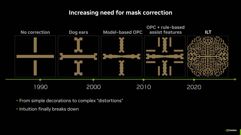 As chipmaking required finer and finer features, engineers had to produce more and more complex designs to project those features onto the silicon. Inverse lithography (ILT) is the latest development.Nvidia
The long computation time for lithography slows the development and improvement of chip technology Even a change to the thickness of a material can lead to the need for a new set of photomasks, notes Vivek K. Singh, vice president in the advanced technology group working on silicon manufacturing at Nvidia. Computing masks “has been a long pole in chip development,” he says. “If inverse lithography technology were sped up 40 times, would more companies use it on more layers? Surely.”
Part of the computation is an image problem that’s a natural fit for GPUs, says Singh. But at most, that can only cut the computation time in half. The rest is not so easy to make parallel. But over the past four years, with development partners including TSMC, Nvidia engineers have come up with a collection of algorithms for making the remaining work parallel and have packaged it as a software library for use with GPUs.
According to Nvidia, using the cuLitho lets 500 Nvidia DGX H100 computers do the work of 40,000 CPU systems. It can produce three to five times as many photomasks per day, drawing only 5 megawatts instead of 35 MW.
What’s more, the technology may deliver better results, according to Singh. CuLitho produces otherwise hard-to-calculate curvy polygons on the mask, which results in a greater depth of focus for the pattern cast onto the wafer. That depth of focus should lead to less variation across the wafer and therefore a greater yield of working chips per wafer, he says. In future, it also could mean fewer photomasks are needed; with inverse lithography, what must now be done with a double pattern might work with only one.
Nvidia is not the first to look to GPUs to accelerate inverse lithography technology. Silicon Valley-based D2S announced a GPU-based computer custom built for the problem in 2019. IEEE Spectrum reached out to D2S for comment, but the company did not reply before press time.
- Custom Computer Makes Inverse Lithography Technology Practical for First Time ›
- Nvidia Announces GR00T, a Foundation Model For Humanoids - IEEE Spectrum ›