If you were a reader of IEEE Spectrum in 2023 with an interest in semiconductors, this list of the top stories says some interesting things about you. For instance, you liked scandal and speed. But you’re also a discerning and forward-looking person. You wanted to know what the future of Moore’s Law is and who would be making it happen. You also wanted to know how semiconductors will play a part in combating climate change.
We’re already giving you a taste of the next year in semiconductors, and we can’t wait to see what you read most in 2024.
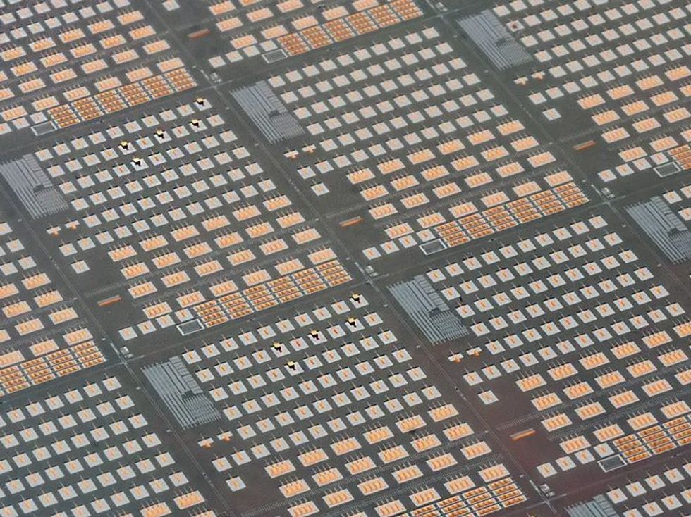
1. Ending an Ugly Chapter in Chip Design
 Chung-Kuan Cheng et al.
In 2022, a schism in the chip design world and at Google erupted into the open. At issue was a reinforcement-learning AI system that Google uses to do a key step in laying out chunks of logic and memory for its AI accelerator chips, or TPUs. In research published in Nature in 2021, Google claimed it beat top academic algorithms and human chip designers at finding the optimal layouts. A rival group at Google responded that it didn’t, but the company wouldn’t publish the rival’s results. When a version was leaked ahead of a major conference, things got ugly.
A year later, a group led by IEEE Fellow Andrew Kahng reported research he said was meant to get the community past the unpleasant episode. Kahng’s research largely backed the rival group’s take on things. It has since led to an editorial expression of concern from Nature, and Kahng has retracted the editorial that originally accompanied Google’s paper. But the search giant still backs its AI. As recently as August 2023, Jeff Dean, chief scientist at Google DeepMind, said that compared to other methods the TPU team had available, 26 of the TPU’s 37 blocks had better performing layouts because of the AI, and 7 of 37 performed equally well.
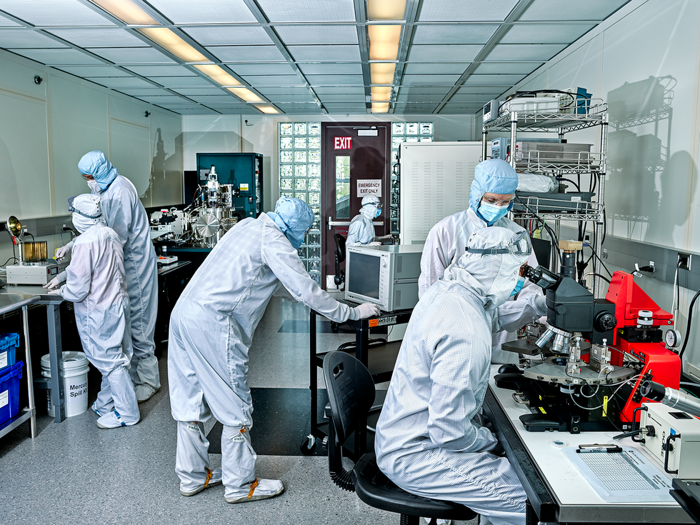
2. U.S. Universities Are Building a Semiconductor Workforce
 Peter Adams
With the U.S. CHIPS and Science Act set to pump tens of billions of dollars into chip manufacturing in the United States, the question has come up: “Who is gonna work in these new fabs?” As long-time contributor Prachi Patel reports, universities across the United States, especially those near fab construction projects, are revamping their semiconductor education offerings in response. The hope is to steer talented students away from the allure of AI and other hot fields and steer them toward making the chips that make AI happen.
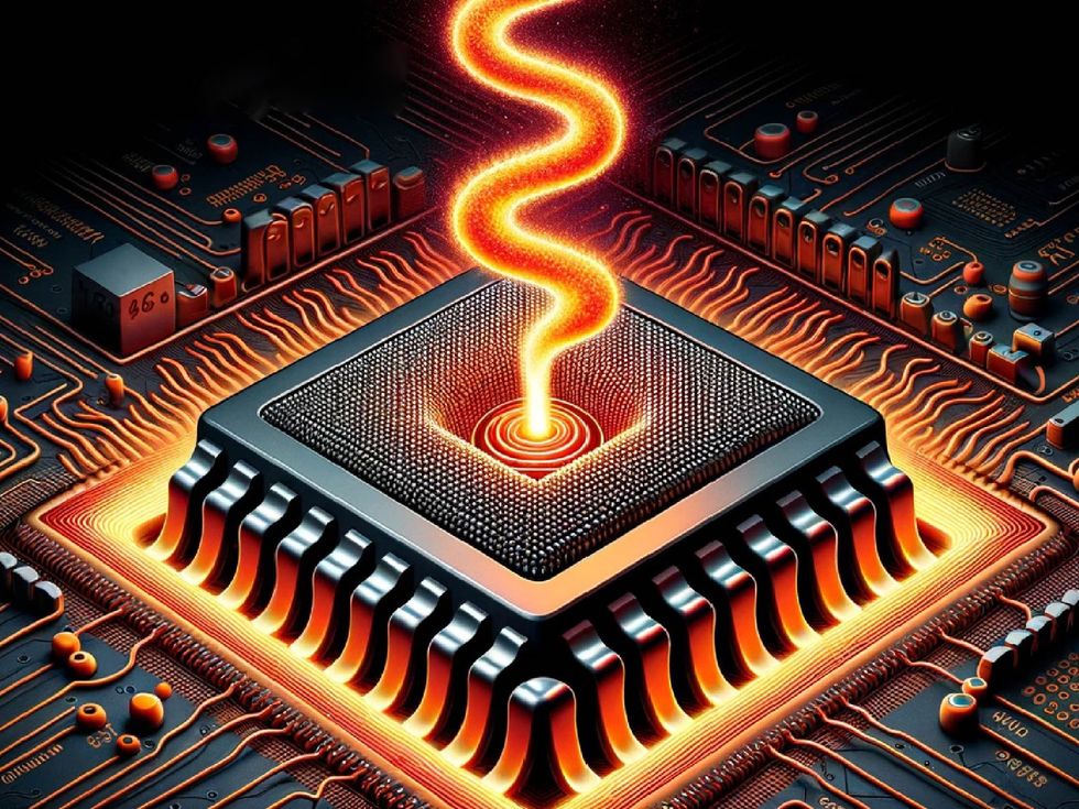
3. Thermal Transistors Can Handle Heat With No Moving Parts
 H-Lab/UCLA
In November, researchers from University of California, Los Angeles reported the invention of a thermal transistor, the first solid-state device that uses an electronic signal to control the flow of heat. Heat removal has been a long-standing limit on processor performance, and it’s only going to get more difficult as processors become collections of 3D-stacked chiplets. Even today’s advanced methods are slow to react to changes in chip temperature when compared to a thermal transistor, which can switch heat conductance on and off as quickly as 1 megahertz.
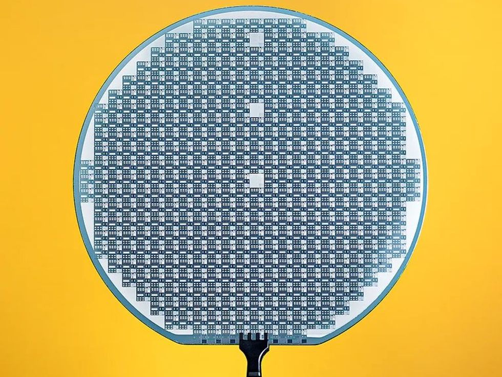
4. Inside the Moore’s Law Machine
 ASML
ASML
Extreme ultraviolet lithography was decades in the making, only entering regular service a few years ago to print nanometer-scale patterns on the most advanced chips. It’s already time for an upgrade. As engineers at ASML explained in Spectrum‘s August issue, the version of the technology in use now is limited to making patterns with a resolution of about the wavelength of its light, 13.5 nanometers. To get below that limit, engineers had to make some major changes to the system’s optics and fix all the knock-on problems that followed. Incidentally, this isn’t the only improvement to EUV coming. New technology, resembling a fuel cell operating in reverse, will make the technology greener. You can hear about both in this episode of IEEE Spectrum’s Fixing the Future podcast.
5. Gallium Nitride and Silicon Carbide Fight for Green Tech Domination
 Peter Adams
We worry more and more about the carbon footprint of semiconductor manufacturing, but this story was actually a win for the climate. Silicon carbide and gallium nitride power semiconductors are both more efficient than their silicon counterparts. The question IEEE Spectrum sought to answer was: Which of these wide bandgap semiconductors works best when? The answer is complicated but fascinating. One thing is clear, both these semiconductors will keep a lot of carbon from entering the atmosphere.
6. Intel Is All-In on Back-Side Power Delivery
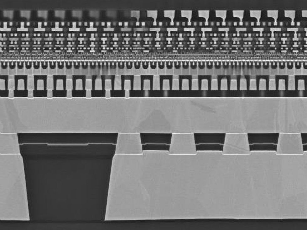
Chipmakers plan a big change in the architecture of interconnects in high-end processors. Since the IC was invented, all of the metal that connects transistors was formed above the silicon surface. That’s worked well for decades, but it’s going to have to come to an end. There’s a fundamental tension between what data-carrying interconnects need and what power-carrying interconnects want. Basically, less power is lost if the interconnects carrying it are short and wide. So researchers hatched a scheme to move the power delivery network to the underside of the silicon, where metal lines could be kept broad and conductive. That leaves more room to better pack in the data-carrying lines above. Intel was the first chipmaker to announce that it would manufacture chips using back-side power delivery, a tech it calls PowerVia. In June, the company shared results showing that, on its own, PowerVia leads to about a 6 percent performance boost, which is about half what you typically get from a major scale down of transistors. Intel will be making a CPU using the combination of PowerVia and new transistors it calls RibbonFETs in 2024.
7. 4 Ways to Put Lasers on Silicon
 Emily Cooper
Silicon is great for lots of things. Making lasers is not one of them. But having a laser on a silicon chip solves a lot of awkward integration problems that could help speed data between processors and other chips. So engineers have been coming up with practical ways to integrate lasers made of compound semiconductors onto silicon wafers, and do it in a way that’s manufacturable and relatively cheap. We showed you four of them, ranked from the most mature to the farthest out.
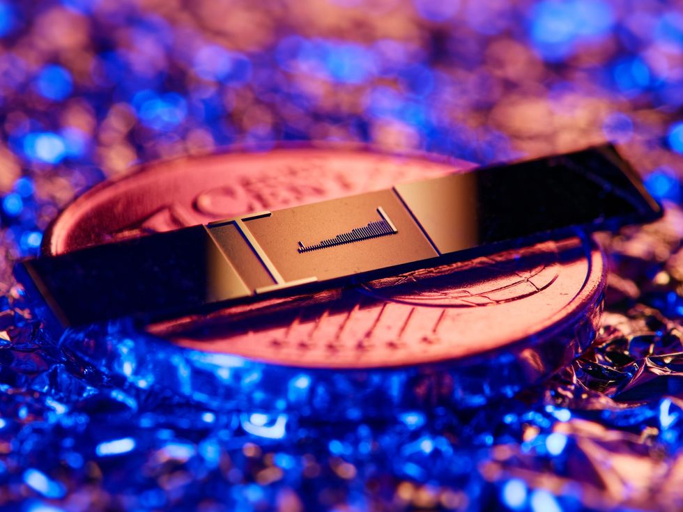
8. Particle Accelerator on a Chip Hits Penny-Size
 FAU/Laserphysics/Litzel/Kraus
Few technologies have versions that are both the size of a city and the size of small coin. But now particle accelerators can make that claim. Instead of using electric fields to boost the speed of electrons along a long track, scientists in Germany used light to zip them through a groove just nanometers wide and 0.5 millimeters long. At that scale the electric field that speeds the electrons along comes from the light’s oscillating electric field. Electrons went 40 percent faster under the accelerator’s influence. The scientists hope they can someday zap them to speeds useful for medical research and other applications.
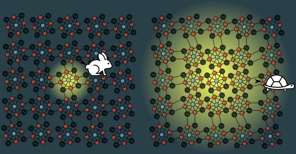
9. Researchers Uncover the Fastest Semiconductor Yet
 Jack Tulyag/Columbia University
What has 6 rhenium atoms, 8 seleniums, and 12 chlorines? The fastest semiconductor yet discovered, that’s what. This molecule forms superclusters that act like one big atom but with properties no single one of those elements has. The secret to its speed lies the behavior of phonons, quasiparticles formed from vibrations in a solid. Usually phonons slow things down, in part by interfering with excitons, bound pairs of electrons and positively charged holes. Instead of knocking excitons around, phonons in this molecule bind to them to create a new quasiparticle that flow freely through the semiconductor at twice the speed of electrons. Too bad rhenium is one of the rarest elements on Earth.
10. The Practical Power of Fusing Photons
 Chad Hagen
Silicon solar cells are relatively cheap and plentiful, but they miss out on a lot of energy in sunlight. Basically, no color of light with an energy less than silicon’s bandgap gets used. But what if we could turn those colors into silicon’s preferred hues? Researchers at Stanford explained just how that’s done. Through a complicated process of exchanging electrons between multiple molecules and energy states, they’ve found a way to turn two useless photons into one useful one. The implications for photovoltaics could be enormous.