Gregory Erickson, Founder and CFO of General Graphene Corporation, details the properties of graphene that make it a versatile and sought-after material.
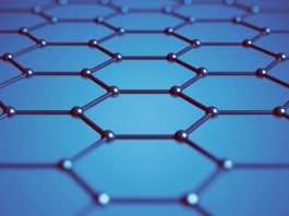
Graphene has long been touted as ‘the next big thing’ in the world of materials science since it combines high electrical conductivity, impermeability, biocompatibility, high thermal conductivity, and strength into a material that is transparent, chemically inert, under a nanometre thick, and weighs less than a milligram per square metre.
At the nanoscale, graphene is the strongest, thinnest, and most conductive material known, which is why most people see graphene as the solution to a diverse array of problems. However, our fundamental belief is that the versatility of graphene can only be harnessed when it is combined with other materials to create novel solutions that utilise the properties of graphene to deliver superior performance in various areas.
By pairing graphene with existing materials, we aim to accelerate its transition from the ‘next big thing’ to the ‘current big thing’ in the materials science world.
The carbon family
Ever since its discovery, people have viewed graphene as one material but, in truth, graphene is a spectrum of carbon-based materials. The properties of graphene change as the number of graphene layers is increased, crystal structure and alignment are changed, doping agents are introduced, and different substrates are employed.
Just as carbon comes in many familiar – yet very different – forms, such as diamond and graphite, so too does graphene. By tuning or manipulating the graphene to emphasise specific properties and pairing it with other materials, we can effectively create a wide range of very different materials, all of which – or none of which – might be referred to as ‘graphene’. At the nanoscale, carbon exists in the form of nanotubes and graphene. Going beyond the nanoscale into the microscale, carbon can also compose of structures which lack crystallinity – these are known as amorphous carbon materials.
Our proprietary atmospheric pressure chemical vapor deposition (APCVD) process allows us to grow graphene and graphene-related carbon materials on a variety of substrates at both the nano and microscale. We discovered that, at the microscale, the resulting carbon growth is closer to a pyrolytic carbon film deposition which ranges from around 100 nm to 10 µm in thickness.
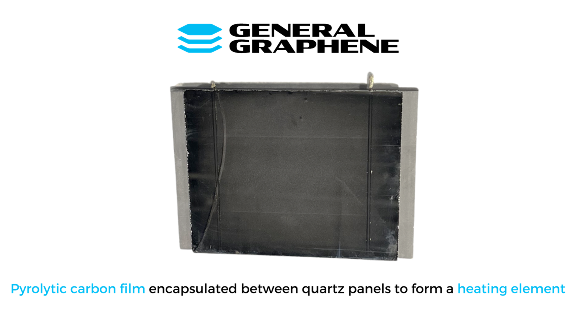
These films exhibit graphitic behaviour and have a unique set of properties:
- Low resistance (1-100 Ω/sq undoped);
- Opaque;
- Uniform, conformal coating;
- Robust and abrasion resistant;
- Stable at high temperatures (1,000°C in an inert environment); and
- Uniform, isotropic heat distribution.
With traditional chemical vapor deposition, the growth of graphene is limited to a select group of metallic films that serve as a catalyst for the separation or cracking of the carbon source. In contrast, pyrolytic carbon films can be deposited directly on a variety of high-temperature compatible substrates.
Some potential applications of these pyrolytic carbon films include:
- Heating elements;
- Heat spreaders;
- X-ray detection windows; and
- Inert biocompatible coatings.
Harnessing graphene’s versatility: The process
Graphene’s unique combination of properties offers exceptional potential with respect to a diverse group of both applications and industries. While this potential is real, in order for it to be realised, it is important to recognise that graphene is not a ‘one-size-fits-all’ material. Its properties are dependent on a variety of factors, including the type of graphene being produced (single or multi-layer), the process parameters being used, and the quantity of inputs being deployed, to name a few.
We realised early on that, to fully harness graphene’s versatility, we would require a production process that can make graphene with a consistent reproducible quality for any given application in a cost-effective and scaleable manner. Our experienced science team has developed hundreds of recipes designed explicitly to meet the requirements of the application. Ultimately, the commercialisation of graphene-based applications is a function of two questions: does it perform/work and is the cost reasonable?
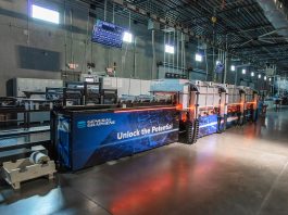
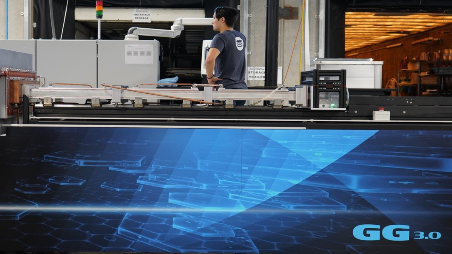
Our engineering team developed GG 3.0 – our novel, industrial-scale, atmospheric pressure chemical vapor deposition (APCVD) production system. Combining mass production with our innovative, high throughput graphene transfer systems allows us to grow and transfer graphene faster and more efficiently onto a wider set of substrates than ever before.
Through the careful amalgamation of science and engineering, we have created a process that allows us to tailor graphene’s properties to fit various applications. We are confident that continued production process innovation and optimisation will enable us to extract the full potential of graphene’s versatility and deploy it cost-effectively – and perhaps more importantly, at commercial scale – across a broad range of applications.
What is next?
If we look at the silicon wafer industry, the market value of silicon wafers as a standalone material in 2018 was roughly $9bn. In contrast, the market value for smartphones enabled by silicon chips in 2018 exceeded $500bn – the factor difference being more than 55 times.
We believe that graphene holds a similar power as an enabling material (it is no coincidence that carbon and silicon are neighbours on the periodic table). Graphene can both enhance today’s products and technologies and facilitate the development of the products and technologies of the future. This is why General Graphene’s core focus has always been myopic in nature: to unleash graphene’s potential we must first demonstrate the ability to mass produce low-cost graphene at a consistent and reproducible quality.
We have done that, and now we are ready to lead the graphene revolution. Our graphene works, and it is significantly cheaper than what other players in the graphene market can provide.
Please note, this article will also appear in the eleventh edition of our quarterly publication.