
In this article we will understand the most important topic about the design of bootstrap high side gate driver circuit but before that lets understand its application.
When it comes to transfer of high power from one voltage level to another voltage level for example conversion of high voltage 400V to low voltage 12V and lets say 3kW of power, we need switching converter that can do the job efficiently and effectively.
However to use the switching converter we need some isolated topology (as the voltage levels are different on input and output) for example Phase shifted full bridge or PSFB which requires mosfet as a switching device.
But to drive the NPN mosfet for example we need a driver circuit to drive the gate of the N channel mosfet. by the way the for those who don’t know Mosfet full form is Metal Oxide Semiconductor Field Effect Transistor.
Low side Gate Driver Mosfet Circuit
It is easy to drive the mosfet on the lower side which is also referred to as low side mosfet, reason being the ground of driver power supply pin VDDB which is GNDB is same same as source of bottom side mosfet. So the close loop is formed between gate, source, and power supply. we can understand more clearly with help of below low side gate driver circuit.
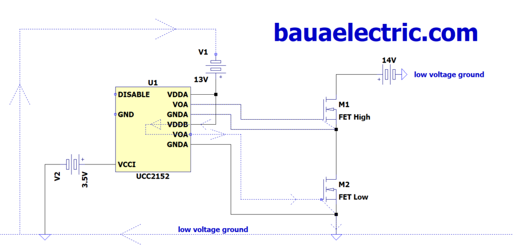
as you can see the arrow in dotted line how it flows to make the gate to turn on, so the arrow reflects the turn on path, there is a circuitry for on and off for the gate of Mosfet, but for the sake of simplicity it is not shown here. The current in this case takes a close loop path, which is not in the case of High side switch we will understand that too in detail.
High Side Gate Driver Mosfet Circuit
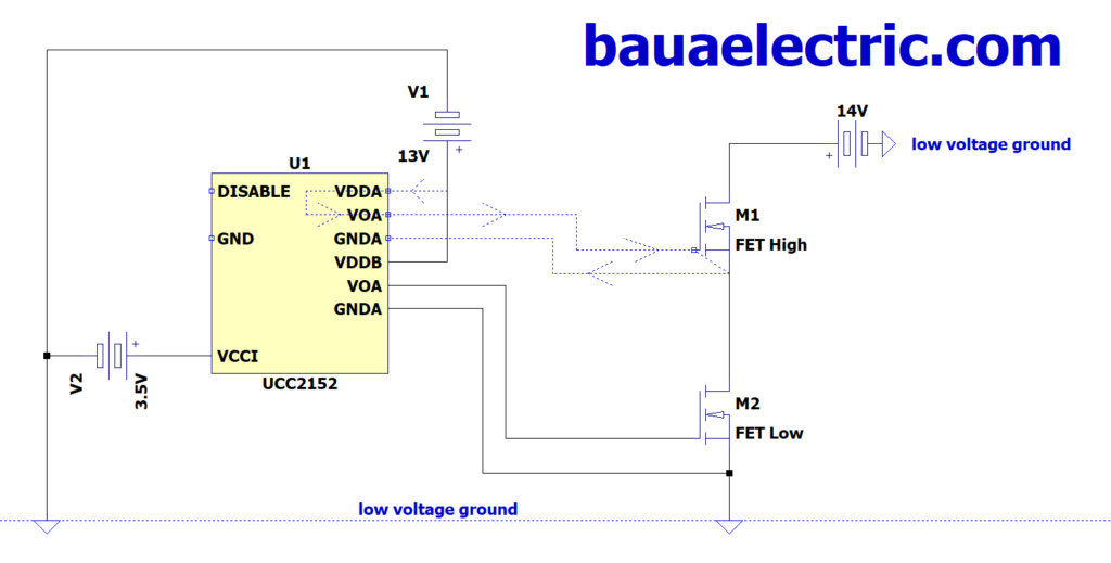
As you can see in the picture high side gate driver circuit current path is shown in dotted line, it clear that the source of the high side power mosfet is not connected to the power supply ground therefore current cannot find a close loop to flow. hence we need a separate solution to drive the top side of power Mosfet.
Hence here comes a Bootstrap circuit concept which is the most easy method. there are other options too which can be considered as an alternate of bootstrap circuit such as separate power supplies with different grounds for all the switches which can be generated using Auxiliary power supply, we can also use current transformer. so now lets understand what is Bootstrap gate driver circuit and how to design it ?
Bootstrap Circuit design
Driving high side Mosfet using bootstrap circuit is the easiest, reliable and safe method. let us understand in detail about this methodology.
So, what exactly is bootstrap circuit and what does it looks like ? the answer lies in the circuit diagram given below.
Capacitor Charging
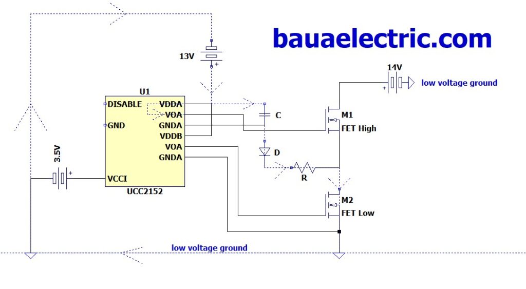
The diagram shows the charging path of the bootstrap capacitor C. the capacitor is charged when the low side Mosfet is turned on. current flows through bootstrap capacitor, diode (D), current limiting resistor and low side FET and than through gate driver IC power supply.
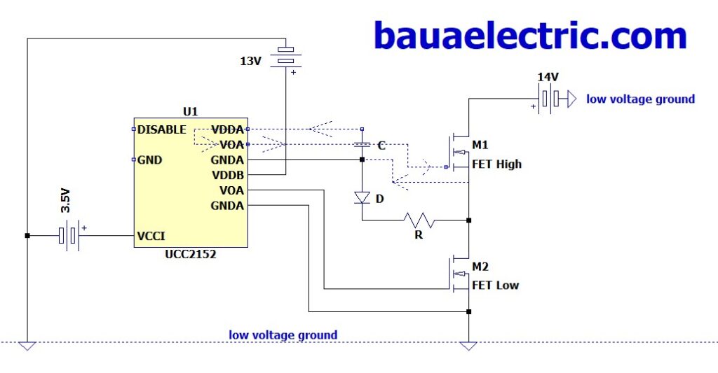
Capacitor discharging
Components Selection
Before starting the design of the components let us first understand the purpose of each components in the circuit. Resistor R is used for limiting the current caused by the charging of bulky bootstrap capacitor as it creates a surge in the current in the start of the charging cycle.
Diode D is used for the unidirectional operation i.e. to prevent capacitor C supplying in reverse order to the power supply.
Bootstrap Capacitor
C_g = Q_g/V_g
where Q_g is the gate charge which is easily available in Mosfet datasheet, and V_g is the voltage appearing at gate to source of high side mosfet.
V_g = VDD – V_fwd
VDD is the voltage of the power supply and V_fwd is the forward voltage drop of diode.
C_boot > 10*C_g the reason being is to prevent any failure due to low gate to source voltage, supply sufficient voltage to gate such that C_boot should not get discharge easily.
Note: Voltage appearing at the gate of mosfet should be greater than UVLO of the driver IC in all worst case scenario.
Bootstrap Diode
Bootstrap diode selection should be done in such away that it should provide
- minimum forward voltage drop as possible
- minimum reverse recovery loss
- temperature rise should be minimum
- recommended to be a fast diode or schotky diode
Bootstrap Resistor
as soon as resistor is added in series with capacitor there exist a delay in charging the capacitor this delay is called the time constant of the circuit, The total delay is 5*R*C seconds to fully charge a capacitor therefore this delay should not be to high as due to high resistor capacitor will not be able to charge to full voltage. Hence the time constant is a one deciding factor. the relation holds like T = R*C/duty cycle
and for energy dissipation due to charging current the relation holds like this, E = 0.5*C_boot*Vgs^2
Resistor should be able to withstand the power dissipation due to the surge in the capacitor charging current which is I_c = C*dv/dt
maximum peak current that capacitor will see is I_pk = (VDD – Vfwd )/Rboot
Layout Considerations for Bootstrap circuit components placement
in order to minimize parasitic inductance and reduce high current trace length it is important to carefully place these components and keep the current loop as small as possible. The bootstrap capacitor and bypass capacitor should be placed as closed as possible to the gate driver supply pins. It is also important to separate high voltage power and low voltage signal traces.
Conclusion
now we came to end of the topic and lets summarize what we saw and covered till now. we discussed the significance of dicrete power mosfet and gate driver circuit.
We also understood the difference between high side and low side Mosfets and why their gate driver circuits are different form each other.
We also looked why we need bootstrap gate driver circuit and its charging and discharging current path and also how to design the components involved in the bootstrap circuit. we also looked on to the layout considerations of the circuit.
1. what is bootstrap gate driver circuit ?
bootstrap driver circuit is used to turn on the high side Mosfet in any SMPS device. it involves the use of R,C,D circuit where C is called as bootstrap capacitor, diode and resistor.


Hello, great article, would you know the possible reason a bootstrap diode keeps shorting briefly after the power supply starts up successfully?
Regards David
can you please share more details about the which power supply or may be some block diagram